Wio-LR2021 Introduction
1. Introduction
The Wio-LR2021 Wireless Module is a next-generation, multi-band wireless transceiver module powered by Semtech's fourth-generation LR2021 chipset. It integrates Sub-GHz (863-928MHz), and 2.4GHz ISM operation into a single compact subsystem, eliminating the need for multiple radio designs across regional and application boundaries.
Designed for IoT developers, LPWAN solution providers, asset tracking engineers, smart agriculture system integrators, and industrial IoT product managers, the Wio-LR2021 bridges the gap between ultra-long-range Sub-GHz communication and high-speed 2.4GHz data links, enabling developers to build globally deployable products without maintaining multiple RF hardware variants.
2. Features
2.1. Unified Multi-Band RF Architecture
The Wio-LR2021 integrates multiple distinct RF bands into a single compact subsystem. Sub-GHz coverage (863-928MHz) ensures compliance with regional unlicensed bands worldwide, while 2.4GHz ISM operation provides higher data rates and global harmonization.
The Semtech LR2021 chipset employs a Switchless Direct-Tie matching network architecture that eliminates the need for external RF switches. PA output and LNA input share the same RF node on the Sub-GHz port, reducing BOM count and board complexity. When transmitting above +6dBm, additional front-end protection is required; absolute maximum input is +10dBm.
The module’s RF interface has a maximum input power of +10dBm; exceeding this may cause irreversible damage. We recommend adding extra protection to the RF front end when input power exceeds +6dBm. Please take special care when using the module near high‑power transmitters.
2.2. Ultra-Low Power Design
With a deep sleep current of just 583nA and idle current of 960uA, the Wio-LR2021 is optimized for battery-powered and energy-harvesting applications.
For maximum battery life, utilize the Warm Sleep mode which retains DIO configuration across wake cycles.
| Mode | Current | Conditions |
|---|---|---|
| TX (868MHz, +22dBm) | 116.0 mA | Sub-GHz maximum power |
| TX (915MHz, +22dBm) | 119.4 mA | Sub-GHz maximum power |
| TX (2.4GHz, +12dBm) | 28.4 mA | 2.4GHz maximum power |
| RX (Sub-GHz, LoRa SF12/125kHz) | 8.19 mA | Maximum sensitivity mode |
| RX (2.4GHz, LoRa SF12/125kHz) | 8.59 mA | Maximum sensitivity mode |
| Deep Sleep | 583 nA | All functions off, configuration retained |
| Idle / Standby | 960 uA | RC oscillator running, register retention |
2.3. Advanced Modulation and Protocol Support
The module supports an extensive range of modulation schemes: LoRa for long-range LPWAN, FLRC (Fast Long Range Communication) for high-speed links up to 2.6Mbps, (G)FSK and (G)MSK for legacy compatibility, 4-FSK and O-QPSK for standardized protocols, and LR-FHSS for robust satellite IoT connections.
Native hardware support enables software-defined migration between LoRaWAN, BLE 5.0, IEEE 802.15.4 (Thread/Zigbee), Wi-SUN, Wireless M-BUS, and Amazon Sidewalk without hardware changes. This future-proofs designs against evolving standards and regional requirements.
2.4. High-Speed FLRC for Multimedia Streaming
FLRC modulation enables data rates up to 2.6Mbps — far exceeding traditional LoRa capabilities. This makes the Wio-LR2021 suitable for applications requiring video preview, audio streaming, or bulk firmware updates over wireless links that still benefit from LoRa's ranging and robustness characteristics.
2.5. World-Class Receive Sensitivity
The Wio-LR2021 achieves -141.1dBm sensitivity at Sub-GHz SF12/125kHz bandwidth, enabling link budgets exceeding 160dBm in favorable conditions. At 2.4GHz, sensitivity reaches -133dBm at SF12/400kHz, outperforming most competing dual-band solutions.
2.6. Compact SMT Package with Pre-Certification
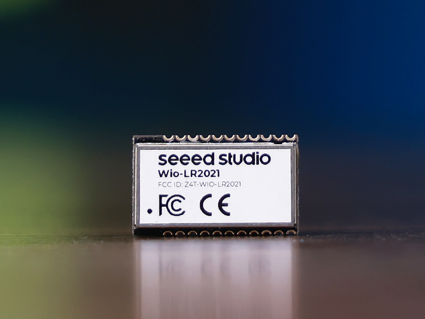
Measuring just 17.07x10.42x2.8mm in a 22-pin SMT package, the Wio-LR2021 minimizes board space while maximizing capability. FCC and CE pre-certification status reduces time-to-market by simplifying the host device certification process.
The Wio-LR2021 is a pure RF transceiver module with no integrated application processor. It requires an external host MCU (such as STM32, nRF52, ESP32, or RP2040) for control via SPI interface.
3. Hardware Overview
3.1. Schematic Diagram
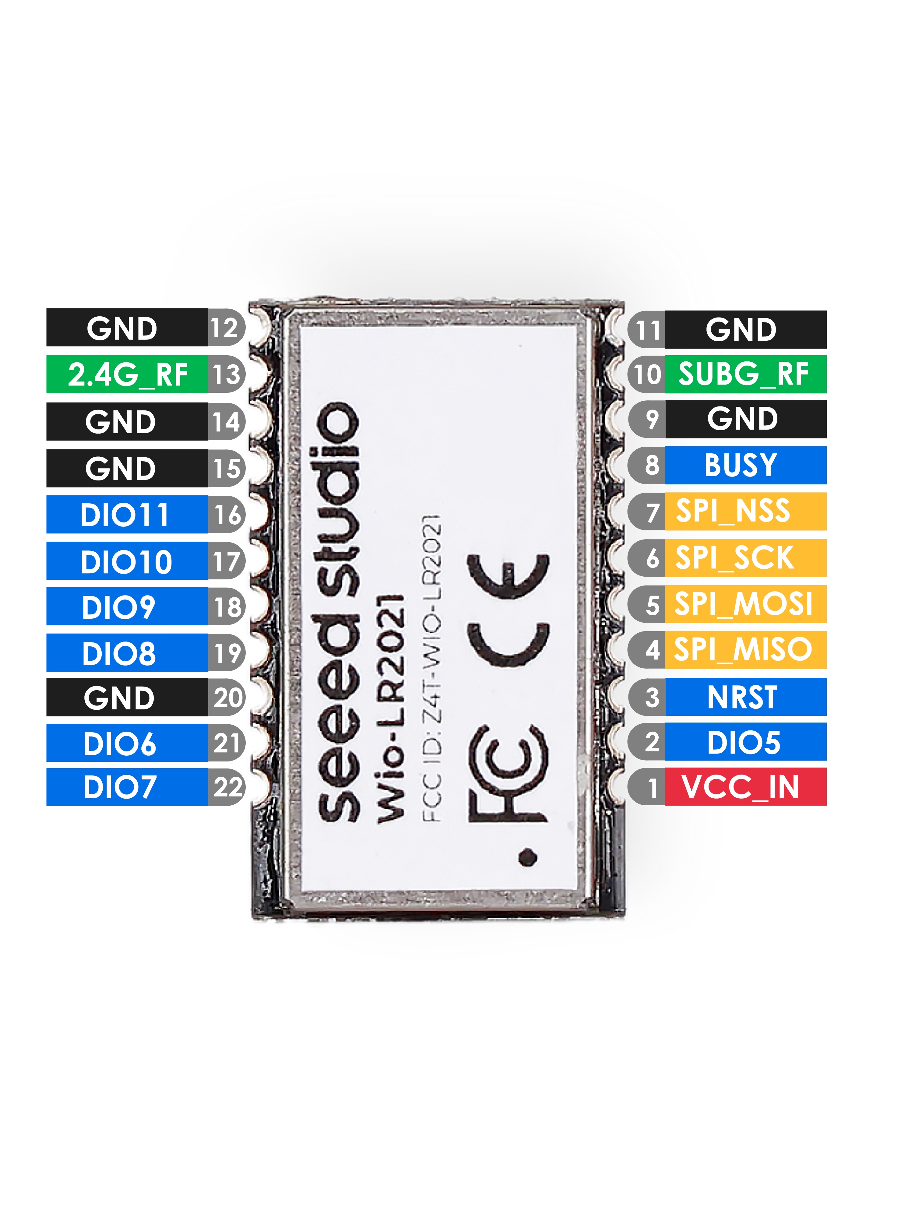
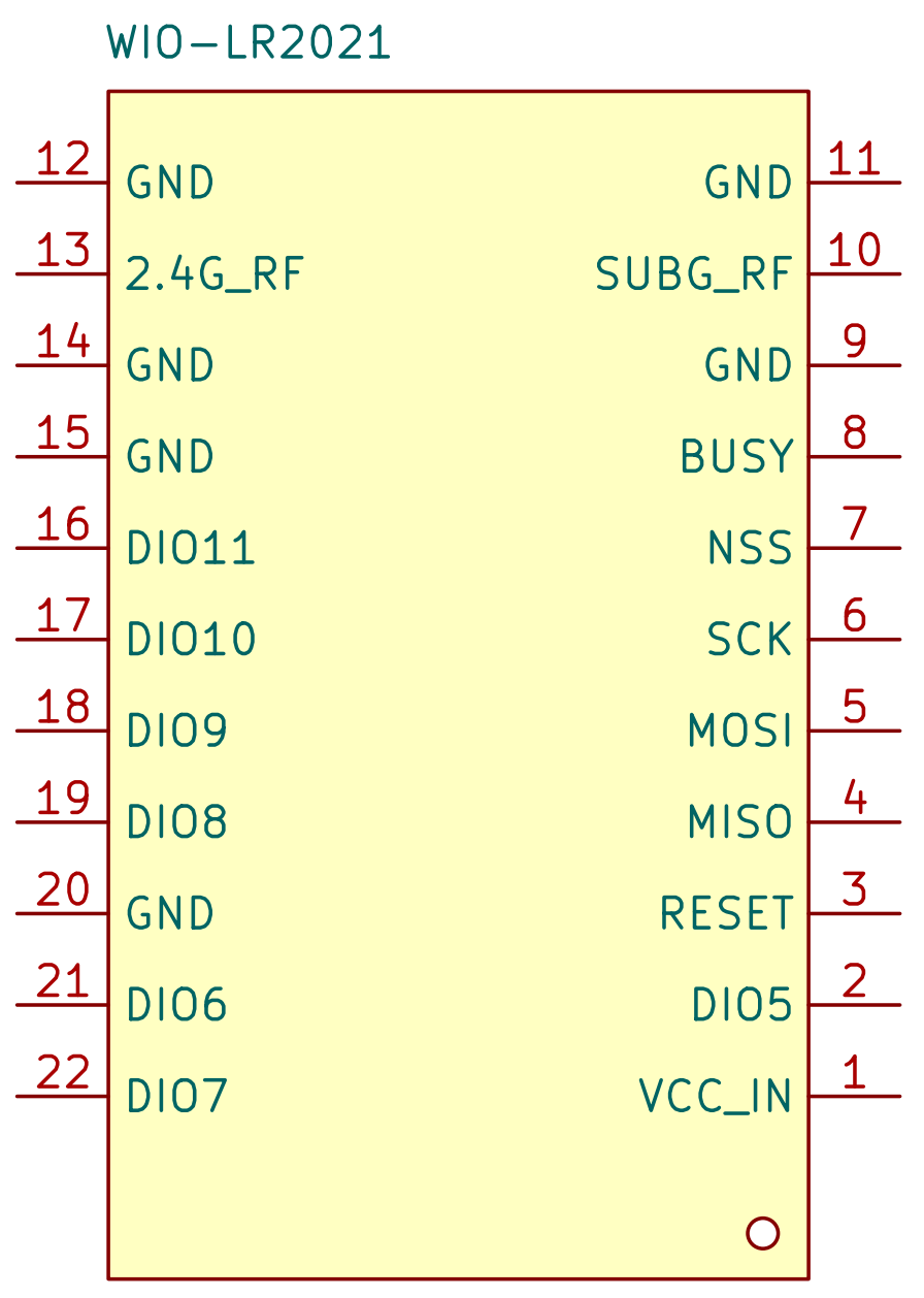
3.2. Pinout
| Pin Number | Pin Name | Type | Description |
|---|---|---|---|
| 1 | VCC_IN | Power Input | 1.8V - 3.7V supply input |
| 2 | DIO5 | Digital I/O | IRQ, RF switch control, clock output, Internal weak pull-up to VCC_IN at reset |
| 3 | RESET | Digital Input | Active LOW |
| 4 | SPI_MISO | Digital Output | 3.3V logic, Hi-Z when NSS de-asserted (HIGH) |
| 5 | SPI_MOSI | Digital Input | 3.3V logic, Hi-Z when NSS de-asserted (HIGH) |
| 6 | SPI_SCK | Digital Input | Max 16MHz, Mode 0 (CPOL=0, CPHA=0). |
| 7 | SPI_NSS | Digital Input | Active LOW |
| 8 | BUSY | Digital Output | Open-drain output, external pull-up required on host PCB. LOW = ready; HIGH = processing. Auto-pulled HIGH on NSS falling edge. |
| 9 | GND | Ground | Common ground reference |
| 10 | SubG_RF | RF | Sub-GHz RF Pinout |
| 11 | GND | Ground | Common ground reference |
| 12 | GND | Ground | Common ground reference |
| 13 | 2.4G_RF | RF | 2.4GHz RF Pinout |
| 14 | GND | Ground | Common ground reference |
| 15 | GND | Ground | Common ground reference |
| 16 | DIO11 | Digital I/O | High-impedance at reset |
| 17 | DIO10 | Digital I/O | High-impedance at reset |
| 18 | DIO9 | Digital I/O | High-impedance at reset |
| 19 | DIO8 | Digital I/O | High-impedance at reset |
| 20 | GND | Ground | Common ground reference |
| 21 | DIO6 | Digital I/O | Internal weak pull-up to VCC_IN at reset |
| 22 | DIO7 | Digital I/O | High-impedance at reset |
All DIO functions must be configured via SPI SetDioFunction command while in STDBY_RC mode. Configuration is retained across warm Sleep cycles. Plan your host firmware to configure DIOs immediately after module reset.
Resource
-
[STEP] Wio-LR2021 Module 3D Model
Tech Support & Product Discussion
Thank you for choosing our products! We are here to provide you with different support to ensure that your experience with our products is as smooth as possible. We offer several communication channels to cater to different preferences and needs.