Wio-LR2021 PCB Design Guide
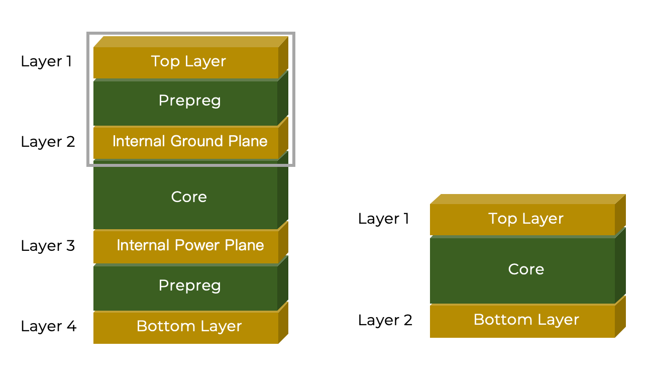
1. Layers
To maximize the available space for RF PCB layout, we recommend using a PCB stack‑up design with four or more layers, particularly in applications with dense routing.
-
For 4‑Layer PCBs, the copper layer immediately beneath the RF area should be designated as a ground plane. The ground plane should be fully populated with copper to ensure continuity of the reference plane.
-
For 2‑Layer PCBs, ensure that the ground plane beneath the entire RF area remains intact wherever possible, and minimize any cuts or splits in the ground plane under the RF trace and components to maintain the integrity of the current return path.
2. Design of a 50Ω RF transmission line
Ensuring that the characteristic impedance of the RF transmission line is 50Ω is the key to RF layout design. Here, we use a Grounded Coplanar Waveguide (GCPW) structure for the RF trace design.
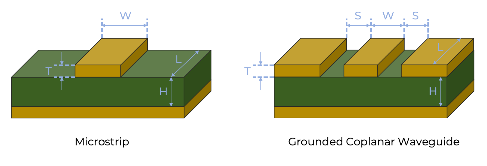
To achieve a characteristic impedance of 50Ω for an RF line using a GCPW structure, the following five key parameters must be determined:
| Symbol | Description |
|---|---|
| S | Spacing between the signal line and the adjacent ground line |
| W | Signal line width |
| T | Copper thickness of the conductor |
| H | Dielectric layer thickness (distance from the signal layer to the reference ground plane) |
| εr | Relative permittivity of the dielectric material |
-
The signal line width W should remain consistent throughout the entire RF path and must not change abruptly.
-
W should match the component pad width as closely as possible If conditions permit, it is recommended to design W to be the same as the pad width of the RF components used to minimize impedance discontinuities (though this is not always feasible).
-
Use free calculation software to help determine 50Ω impedance Free impedance calculation tools (such as AppCAD, Saturn PCB Toolkit, or the impedance calculator in KiCad) can be used to optimize the above parameters, ensuring that the characteristic impedance of the RF lines in the PCB design precisely matches 50Ω.
Here, we will use a standard 0.1mm thick FR4 substrate with 1oz copper cladding as an example to calculate the GCPW (grounded coplanar waveguide) for a 50Ω impedance:
| Parameter | Value(mm) | Remark |
|---|---|---|
| S | 0.199 | Signal line spacing |
| W | 0.190 | RF signal line width |
| T | 0.035 (1oz) | Copper thickness |
| H | 0.1 | Dielectric thickness |
-
Reduced crosstalk and EMI – Compared to conventional microstrip lines or groundless coplanar waveguides, the ground plane on both sides and beneath signal line effectively suppresses crosstalk between adjacent traces or between layers, thereby reducing electromagnetic interference (EMI). This makes GCPW particularly suitable for RF routing in high‑density, multi‑layer PCBs.
-
Improved electromagnetic field confinement – The structure, in which ground planes are placed adjacent to the signal line, significantly confines the electromagnetic field. This reduces the amount of high‑frequency signal energy radiated into the surrounding space, helping to meet electromagnetic compatibility (EMC) requirements.
-
Better impedance stability and tolerance – In a GCPW structure, signal return paths primarily utilize the ground planes on both sides rather than relying solely on the reference ground below. As a result, GCPW offers greater tolerance to manufacturing variations in board thickness(H) and provides more stable 50Ω impedance.
3. RF Routing Guidelines
1. Geometric constraints
1.1. Single‑Layer Continuity
Top layer throughout – From the module's RF pin pads to the antenna mount, matching network, or antenna feed point, the RF trace must be routed entirely on a single layer.
No layer‑change vias – The use of vias to switch layers is prohibited. Vias introduce inductive discontinuities (typically 0.5–1.5nH), which can cause significant impedance jumps and degraded return loss.
If a layer change is unavoidable (not recommended and only under extreme space constraints), the following must be observed:
Place a coplanar GND via array (at least four vias, symmetrically distributed around the signal via) at the layer transition point.
1.2. Constant Trace Width
The trace width (W) and the gaps (S) on either side must remain constant along the 50 Ω characteristic impedance section, from the module's RF pins to the antenna port.
1.3. Minimise Trace Length
Sub‑GHz bands (433/868/915 MHz): The total length of RF traces is recommended to be ≤ 20 mm. Exceeding this length results in a significant increase in transmission line loss and parasitic radiation.
2.4 GHz band: Recommended ≤ 30 mm. If exceeded, the loss budget of the matching network must be reassessed.
The total length includes the trace from the module pin pad exit through the matching network to the centre pin of the antenna socket, excluding the interior of the antenna socket and the antenna body itself.
1.4. Bending Rules
- 90° right angles are prohibited.
- The bend radius must be at least three times the trace width(W), with ≥ 5W being optimal. Curved bends provide the smoothest impedance transition in frequency bands below millimetre wave.
- Within a single RF trace, the number of bends should be no more than two.
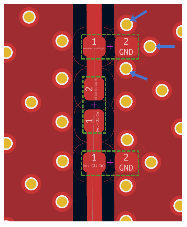
2. Grounding, Shielding, and Via Stitching
2.1. Via Spacing
Along both sides of the RF trace, GND vias are used to short‑circuit the top‑layer coplanar GND to the internal ground plane, forming an electromagnetic shielding wall. The via spacing (D) is determined by the wavelength: D ≤ λ / 20
| Operating Band | Center Frequency | λ/20 (Theoretical Value) | Recommended Spacing |
|---|---|---|---|
| EU868 | 868 MHz | 17.3 mm | ≤5 mm |
| US915 | 915 MHz | 16.4 mm | ≤5 mm |
| AS923 | 923 MHz | 16.3 mm | ≤5 mm |
| 2.4GHz | 2400 MHz | 6.25 mm | ≤3 mm |
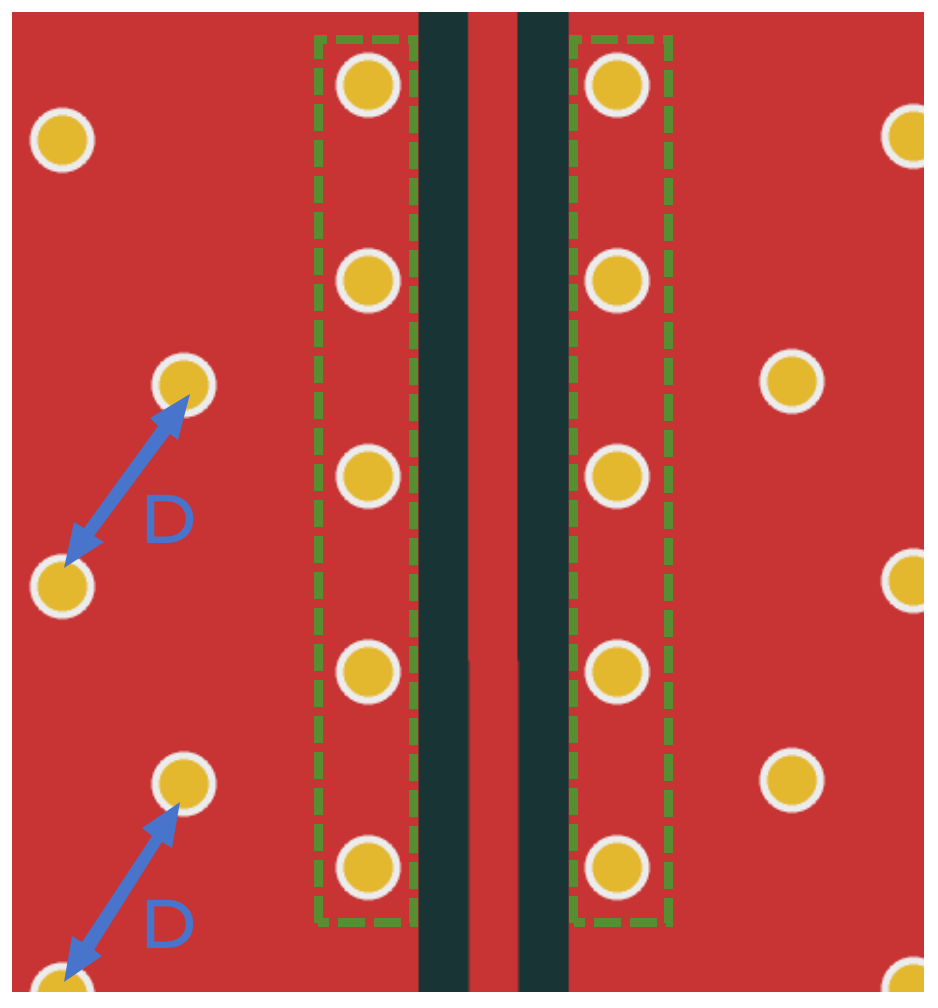
The via spacing used in the design is significantly smaller than the theoretical value in order to suppress higher‑order harmonics and edge field leakage.
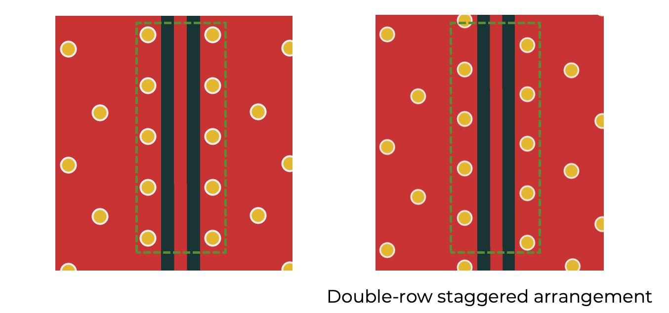
2.2. Via Arrangement
-
Double‑row staggered arrangement is recommended – Place one row of GND vias on each side of the RF trace. The two rows should be staggered rather than directly opposite each other to more effectively block the gap antenna effect.
-
Vias should be placed adjacent to the edge of the RF trace, with a distance of ≤
0.3 mm(i.e., vias should be positioned at the edge of the GND copper layer). -
Recommended via diameter (0.2–0.3mm), to avoid excessive cutting of the top‑layer GND copper layer that can result from overly large vias.
2.3. Edge Stitching
Dense GND stitching via must be placed along the edges of the PCB (especially those containing RF regions) to prevent the board edges from acting as parasitic radiation paths.
3. Reference Planes and Stackup Constraints
3.1. Integrity of the Underlying GND Plane
The layer immediately below the RF trace (Layer 2 in a 4‑layer board, or the bottom layer in a 2‑layer board) must be a complete, uncut GND plane.
3.2. Coplanar Ground Requirements
Coplanar GND copper must be maintained on both sides of the RF trace. The GND edges must be straight and continuous, with no jagged edges or gaps.
The coplanar GND width (F) must satisfy: F > W + G, where W is the trace width and G is the gap between the trace and the GND. If F is too small, the field distribution will shift to the lower layer, causing a change in the effective dielectric constant and a deviation from 50Ω impedance.
3.3. Interlayer Isolation
In a 4‑layer board, power islands on Layer 3 (the power layer) must not be placed directly beneath the RF trace and overlap with Layer 2. If Layer 3 must pass beneath the RF trace, ensure that it crosses the RF trace perpendicularly (to minimize coupling length) and maintain complete ground isolation between Layer 2 and Layer 3.
4. Shunt Components and Matching Networks
4.1. Co‑line Layout
-
All shunt components must be placed directly in series with the RF trace. This means the long side of the component pad aligns with the direction of the RF trace, and the component body “lies” within the RF path.
-
Vertical stubs extending from the RF trace to connect to shunt components are prohibited. Vertical stubs act as open‑circuit stubs; at 868 MHz, even a 5 mm stub can cause significant reflections.
4.2. Ground Vias
-
The ground pads of shunt components must be connected to Layer 2 via at least
threeGND vias, placed as close as possible to the pad. -
Vias should be located close to the edge of the pad and arranged in a triangular or linear pattern to ensure the shortest and most symmetrical ground path.
-
Do not drill vias directly in the center of the component pad. Center vias obstruct solder paste flow during SMT reflow, leading to cold solder joints, and they also increase parasitic inductance.
4.3. Component Orientation and Spacing
-
Multiple shunt components within the same matching network should be arranged sequentially along the RF trace direction to avoid mutual coupling caused by side‑by‑side placement.
-
The recommended spacing between adjacent shunt components is ≥ 1.5× the component length (approximately ≥
1.0 mmfor 0402 packages).
5. Isolation and Spacing
5.1. Isolation from Digital/Power Signals
-
Parallel spacing – The spacing between RF traces and adjacent digital or power traces must be at least
threetimes the trace width (or ≥ 1 mm, whichever is greater). -
Parallel length limit – If the spacing is less than
3 mm, the length of parallel traces must be ≤10 mm. If this length is exceeded, a GND isolation strip (≥ 1 mm wide GND copper patch with via stitching) must be added. -
Vertical crossings – When RF traces cross other signal traces, prioritize perpendicular crossing. The Layer 2 GND must remain continuous beneath the crossing point.
5.2. Isolation from High‑Frequency Interference Sources
RF traces and antenna areas must be kept away from:
- High‑speed clock lines (USB, SPI CLK, SDIO)
- DC‑DC buck inductors and switching (SW) nodes
- Crystal oscillators / TCXOs (even if a TCXO is integrated within a module, other crystal oscillators on the board must still be kept at a distance)
Recommended minimum clearances:
- From DC‑DC inductors: ≥ 20 mm
- From USB differential lines: ≥ 10 mm
- From 32 MHz crystal oscillators: ≥ 15 mm
4. Reference Design
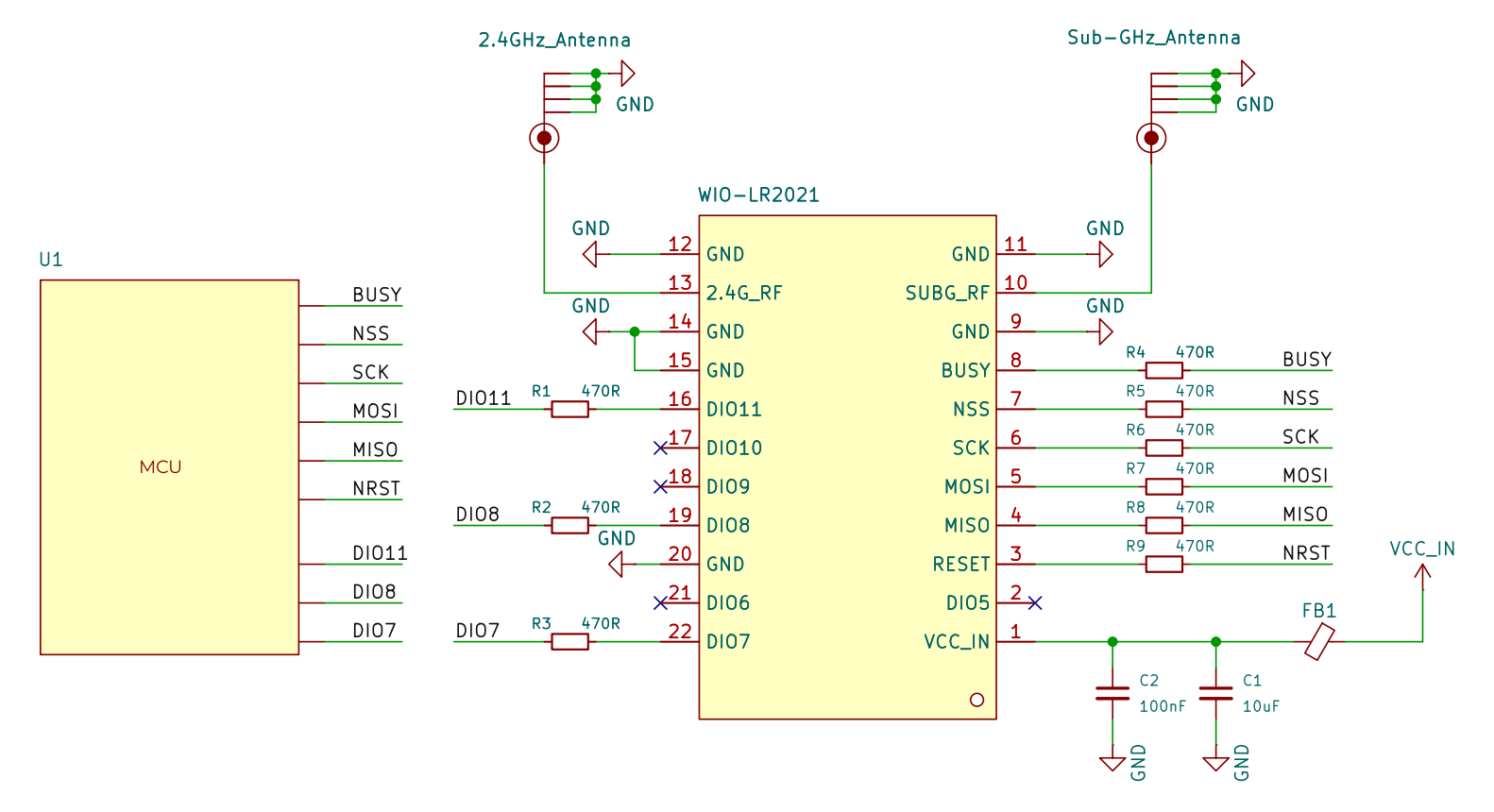
-
Place
C1 (10uF)andC2 (100nF)as close as possible to theVCC_INpin. Poor placement will degrade RF performance and may cause spurious emissions. -
Install
470Ωseries resistors on all SPI lines (NSS, SCK, MOSI, MISO) placed as close to the module as possible for high-frequency harmonic suppression. The module does not support continuous frame mode — NSS must be toggled between commands with minimum 125ns HIGH time.
RF Interface (SubG_RF / 2.4G_RF)
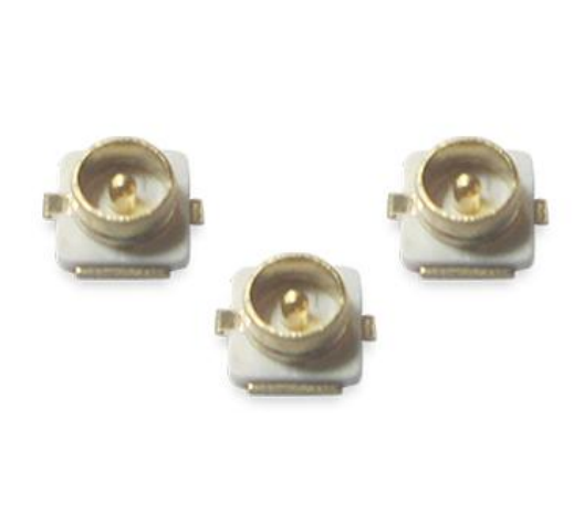
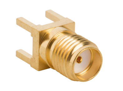
The module provides two independent RF output pins, one for the Sub-GHz band and one for the 2.4GHz band. Internal 50Ω impedance matching has been implemented for both RF paths. We recommend use standard IPEX1 or SMA connector as the antenna interfaces.
Tech Support & Product Discussion
Thank you for choosing our products! We are here to provide you with different support to ensure that your experience with our products is as smooth as possible. We offer several communication channels to cater to different preferences and needs.